Preparation of CuInSe2 Thin Films by Chemical Spray Pyrolysis
Sho SHIRAKATA, Tomonori MURAKAMI, Tetsuya KARIYA1 and Shigehiro ISOMURA
Faculty of Engineering, Ehime University, 3 Bunkyo-cho, Matsuyama, Ehime
790, Japan 1 Faculty of Science, Kochi University, 2-5-1 Akebono-cho, Kochi
780, Japan
(Received August 4, 1995; accept for publication October 17,1995)
CuInSe2 thin films have been prepared by chemical spray
pyrolysis (CSP) on glass substrate from the ethanol aqueous solution containing
CuCl2, InCl3 and N,N-dimethylselenourea. Properties of the CuInSe2 films
(electrical, structural, optical absorption and morphological properties)
have been systematically studied in terms of substrate temperature (Ts),
pH and the ion ratio (Cu/In) of the spray solution. Good chalcopyrite CuInSe2
films with large grains have been grown using the neutralized spray solution
(pH=4) at the growth temperature of 360 . On the other hand, low values
of Ts, pH and Cu/In led to the production of sphalerite films.
KEYWORDS: CuInSe2 thin film, chemical spray pyrolysis, chalcopyrite
semiconductors, CuInSe2/CdS heterojunction
1. Introduction
Copper indium diselenide (CuInSe2:CIS) has a direct band gap of 1.02 eV1) and high
absorption coefficient up to the order of 6 x 105 cm-1.2) Therefore, it is
expected to be a promising material for photovoltaic applications, and is
usually utilized as a solar cell in the form of polycrystalline thin films.3,4)
Recently, the CuInSe2 thin-film solar cells have been reported to attain
very high conversion efficiencies of 16`17 %.5,6) A variety of techniques
have been devised to deposit CuInSe2 thin films.3.4) They include
three-source evaporation, two-stage process (selenization method),
sputtering, chemical spray pyrolysis and electrodeposition. The former two
methods have proven to be promising from the viewpoint of high efficiency,
and therefore most recent studies have focused on them. However, the cost
for the production of the large-area solar cell by these methods is rather high.
On the other hand, chemical spray pyrolysis (CSP) is an attractive method
because large-area films with good uniformity can be grown at low cost. In
this method, gas atomizes the solution containing the constituents into fine
mist with a spray nozzle. The reactant in the droplets is pyrolyzed on the
heated substrate. Ideally, a pyrolysis reaction leads to the deposition of the
films of the desired compound while other products evaporate as gaseous
species. So far, several CSP studies have been done on CuInSe2.7-22) In
spite of its applicability to the fablication of low-cost large-area solar cells,
recent activity on CSP study is low mainly because of the low conversion
efficiency (up to `6%) of the CuInSe2 solar cells with spray films. It seems
that there remain many unknown and uncontrolled factors in CSP which have
not been made clear. The authors have been studying the CSP of CuInSe2
films. Some of the preliminary results of a study on the preparation and
properties of the CuInSe2 films and the CdS/CuInSe2 heterojunction have
already been pubslihed.23) The present study focuses on the relationship
between the properties of the CuInSe2 films and the film-preparation
conditions: (i) substrate temperature, (ii) ion ratio (Cu/In) and (iii) pH in the
spray solution. A series of CuInSe2 films has been deposited on the glass
substrate by CSP from the ethanol aqueous solution containing CuCl2, InCl3
and N,N-dimethylselenourea. CuInSe2 films have been characterized with
respect to X-ray diffraction, surface morphology, Raman spectrum, resistivity
and optical absorption.
2. Experimental
Figure 1 shows the schematic representation of the CSP apparatus used for
the growth of CuInSe2 thin films.
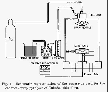 It consists of a bell jar
made of acrylic resin (190 mm in diameter and 250 mm in height), a spray
nozzle of the two-fluid type (IKEUCHI model AK104) and a stainless steel
substrate heater block (60 x 90 x 28 mm3). The distance between the spray
nozzle and the substrate is 215 mm. The spray solution in a dark container
was drawn to the spray nozzle through a flow meter by a roller pump, and it
was sprayed with nitrogen carrier gas onto the heated substrate. The mist
size was about 30 òm. As a spray solution, the 20 volume percent
ethanol aqueous solution of CuCl2, InCl3 and N,N-dimethylselenourea (DMSeU)
was used. For Cu/In=1, the concentrations of CuCl2, InCl3 and DMSeU in the
spray solution were 1.5 x 10⁻³, 1.5 x 10⁻³ and 4.95 x 10⁻³ (mole/l),
respectively, corresponding to the ion ratio of Cu:In:Se=1:1:3.3. The
concentration of DMSeU in the solution was in excess of stoichiometry because
Se is more volatile than the other elements. In order to change Cu/In, the
concentration of CuCl2 was changed, keeping concentrations of InCl3 and
DMSeU constant. The pH value in the spray solution was changed between 1.9
and 4.0 by adding NH4OH into the initial solution (pH=1.9). The maximum pH
value used in this study was 4.0, in order to prevent the precipitation of InCl3
and DMSeU in the spray solution because of the high pH value. Prior to the
spray deposition, N2 gas was bubbled through the solution to displace
dissolved oxygen. The growth chamber was purged with nitrogen.
Subsequently, substrate temperature was raised up to the destined value. The
solution of total amount of 250 ml was sprayed with the N2 gas under the
pressure of 2kg/cm2 at a rate of about 5 ml/min. Growth was carried out in
the dark for 50 min. After the growth, substrate was cooled down to room
temperature with a continuous N2 flow. As the substrate, a conventional
glass microscope slide was used. Substrate temperature was between 300
and 360 . Thickness of the CuInSe2 film grown in this way was 0.5`1.5 òm,
corresponding to the growth rate of 10`30 nm/min. The film structure
was characterized by the X-ray diffraction (XRD) method using the Cu-K¢
radiation. Two types of the goniometers have been used: (i) a conventional
goniometer with ó-2ó scanning mechanism, and (ii) a goniometer with a fixed
small-angle X-ray incidence (2Kincidence), and 2ó scanning mechanism with
sample rotation within the plane. The former goniometer was used for
studying orientations of the films with respect to the substrate. The latter
one picks up every diffraction included in the film almost independent of the
film orientation, similar to a powder X-ray technique, and therefore it has
been used for the analyses of the film structure and the second phases.
Observation of surface morphology was performed using a scanning electron
microscope (SEM:JEOL model JSM-5300). Film composition was determined by
an electron probe microanalyzer (EPMA:JEOL model JXA-8600MX) using L¢ line
(for Cu, In and Se) with an acceleration voltage of 7 kV and a beam current of
2.00 x 10⁻⁸ A. The diameter of the electron probe was 10òm. A single
crystal of CuInSe2 was used as the standard which was grown by the normal
freezing method from a stoichiometric melt. The composition was obtained
by averaging the measurements made at ten different points of the same film.
Details of the composition analysis of the CuInSe2 films by EPMA have
already been published.24) The conductivity type was determined by the
hot-probe method. Resistivity was measured by the Van der Pauw method
using evaporated In electrodes. The optical transmission was measured using
a single-beam monochromator (Ritsu Oyo Kogaku, model MC-20l) in
combination with a lock-in amplifier (NF circuit design block, model LI-572B).
Photomultipliers (Hamamatsu R-7102 and R-7696) and a PbS photoconductive
detector were used for the light detection. The optical transmission was
measured together with the glass substrate, and corrected for the absorption
of the substrate. The absorption coefficient was estimated from the formula
(1/d)ln(1/T), with film thickness d and optical transmission T, and
subtracting the minimum value as excess absorption.
It consists of a bell jar
made of acrylic resin (190 mm in diameter and 250 mm in height), a spray
nozzle of the two-fluid type (IKEUCHI model AK104) and a stainless steel
substrate heater block (60 x 90 x 28 mm3). The distance between the spray
nozzle and the substrate is 215 mm. The spray solution in a dark container
was drawn to the spray nozzle through a flow meter by a roller pump, and it
was sprayed with nitrogen carrier gas onto the heated substrate. The mist
size was about 30 òm. As a spray solution, the 20 volume percent
ethanol aqueous solution of CuCl2, InCl3 and N,N-dimethylselenourea (DMSeU)
was used. For Cu/In=1, the concentrations of CuCl2, InCl3 and DMSeU in the
spray solution were 1.5 x 10⁻³, 1.5 x 10⁻³ and 4.95 x 10⁻³ (mole/l),
respectively, corresponding to the ion ratio of Cu:In:Se=1:1:3.3. The
concentration of DMSeU in the solution was in excess of stoichiometry because
Se is more volatile than the other elements. In order to change Cu/In, the
concentration of CuCl2 was changed, keeping concentrations of InCl3 and
DMSeU constant. The pH value in the spray solution was changed between 1.9
and 4.0 by adding NH4OH into the initial solution (pH=1.9). The maximum pH
value used in this study was 4.0, in order to prevent the precipitation of InCl3
and DMSeU in the spray solution because of the high pH value. Prior to the
spray deposition, N2 gas was bubbled through the solution to displace
dissolved oxygen. The growth chamber was purged with nitrogen.
Subsequently, substrate temperature was raised up to the destined value. The
solution of total amount of 250 ml was sprayed with the N2 gas under the
pressure of 2kg/cm2 at a rate of about 5 ml/min. Growth was carried out in
the dark for 50 min. After the growth, substrate was cooled down to room
temperature with a continuous N2 flow. As the substrate, a conventional
glass microscope slide was used. Substrate temperature was between 300
and 360 . Thickness of the CuInSe2 film grown in this way was 0.5`1.5 òm,
corresponding to the growth rate of 10`30 nm/min. The film structure
was characterized by the X-ray diffraction (XRD) method using the Cu-K¢
radiation. Two types of the goniometers have been used: (i) a conventional
goniometer with ó-2ó scanning mechanism, and (ii) a goniometer with a fixed
small-angle X-ray incidence (2Kincidence), and 2ó scanning mechanism with
sample rotation within the plane. The former goniometer was used for
studying orientations of the films with respect to the substrate. The latter
one picks up every diffraction included in the film almost independent of the
film orientation, similar to a powder X-ray technique, and therefore it has
been used for the analyses of the film structure and the second phases.
Observation of surface morphology was performed using a scanning electron
microscope (SEM:JEOL model JSM-5300). Film composition was determined by
an electron probe microanalyzer (EPMA:JEOL model JXA-8600MX) using L¢ line
(for Cu, In and Se) with an acceleration voltage of 7 kV and a beam current of
2.00 x 10⁻⁸ A. The diameter of the electron probe was 10òm. A single
crystal of CuInSe2 was used as the standard which was grown by the normal
freezing method from a stoichiometric melt. The composition was obtained
by averaging the measurements made at ten different points of the same film.
Details of the composition analysis of the CuInSe2 films by EPMA have
already been published.24) The conductivity type was determined by the
hot-probe method. Resistivity was measured by the Van der Pauw method
using evaporated In electrodes. The optical transmission was measured using
a single-beam monochromator (Ritsu Oyo Kogaku, model MC-20l) in
combination with a lock-in amplifier (NF circuit design block, model LI-572B).
Photomultipliers (Hamamatsu R-7102 and R-7696) and a PbS photoconductive
detector were used for the light detection. The optical transmission was
measured together with the glass substrate, and corrected for the absorption
of the substrate. The absorption coefficient was estimated from the formula
(1/d)ln(1/T), with film thickness d and optical transmission T, and
subtracting the minimum value as excess absorption.
3. Results and Discussion
3.1 Film composition
Figure 2 shows the molar
ratio (Cu/In) of the film determined by EPMA plotted as a function of ion ratio
(Cu/In) in the spray solution for films sprayed at pH=1.9 and Ts=300 .
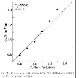 The composition ratio Cu/In in the film almost agrees with that in the solution
for Cu/In between 0.8 and 1.1, and is slightly larger than that in the solution
for 1.2
Cu/In
1.3. This result indicates the excellent controllability of the
film composition by changing the solution composition. Figure 3 shows the
CSP film composition plotted in a ternary composition plane.
The composition ratio Cu/In in the film almost agrees with that in the solution
for Cu/In between 0.8 and 1.1, and is slightly larger than that in the solution
for 1.2
Cu/In
1.3. This result indicates the excellent controllability of the
film composition by changing the solution composition. Figure 3 shows the
CSP film composition plotted in a ternary composition plane.
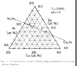 It can be seen that the plots are on the tie line of the Cu2Se-In2Se3 pseudobinary system,
which indicates that the valence stoichiometry is preserved. This result is
similar to that reported for the three-source evaporation method.24) It has
been reported in the In-rich CuInSe2 films prepared by CSP that the excess In
is easily oxidized and it is incorporated in the films as a second phase in the
form of In2O3, especially for low pH solution.18-21) The result shown in
Fig.3 indicates that the inclusion of the In2O3 second phase is negligible. If
films contain much In2O3 phase, plots should be on the left side of the
Cu2Se-In2Se3 tie line. This result is in good agreement with the result
showing the absence of the diffraction line due to In2O3 in the X-ray
diffraction pattern.
It can be seen that the plots are on the tie line of the Cu2Se-In2Se3 pseudobinary system,
which indicates that the valence stoichiometry is preserved. This result is
similar to that reported for the three-source evaporation method.24) It has
been reported in the In-rich CuInSe2 films prepared by CSP that the excess In
is easily oxidized and it is incorporated in the films as a second phase in the
form of In2O3, especially for low pH solution.18-21) The result shown in
Fig.3 indicates that the inclusion of the In2O3 second phase is negligible. If
films contain much In2O3 phase, plots should be on the left side of the
Cu2Se-In2Se3 tie line. This result is in good agreement with the result
showing the absence of the diffraction line due to In2O3 in the X-ray
diffraction pattern.
3.2 XRD study 3.2.1 Effect of substrate temperature
CuInSe2 films have been prepared at various substrate temperatures (Ts) between 300 and 360 with the stoichiometric spray solution (Cu/In=1). Substrate temperature dependence of the XRD patterns for the CuInSe2
films deposited with the unneutralized (pH=1.9) and neutralized (pH=4.0)
spray solution is shown in Figs. 4(a) and 4(b), respectively.
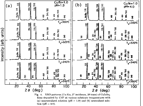 In order to avoid confusion, indexes
for the X-ray diffraction lines in the figures are those of the chalcopyrite
structure. The CuInSe2 films deposited with unneutralized (pH=1.9) solution
at Ts
340 are considered to have the sphalerite structure because they do
not exhibit the diffraction lines (ch-XRD lines) unique to the chalcopyrite
structure. Such ch-XRD lines should be represented by index hkl with odd l,
such as 211. At Ts of 360 , the ch-XRD lines such as 211 and 301 can be
observed. On the other hand, for the CuInSe2 films deposited with the
neutralized (pH=4.0) solution, the ch-XRD lines, 101, 211, 105, 301 etc. can be
clearly seen even for films deposited at Ts=320 and 340 . Further increase
of Ts causes the appearance of the XRD lines 103, 217, 411 and 415.
Therefore, these films are considered to have well-defined chalcopyrite
structure. Raman spectrum from the CuInSe2 film exhibiting the
ch-XRD lines (Ts=320, pH=4.0, in Fig. 4(b)) shows a dominant Raman peak at
175 cm-1 with a weak shoulder at 182 cm-1, as can be seen in the bottom
spectrum of Fig. 5. This peak at 175 cm-1 is assigned to the A1 mode peak,
which is the well-known strong Raman peak in the CuInSe2 crystal with
chalcopyrite structure.25) In contrast, the Raman spectrum of the film
without the ch-XRD lines (Ts=320, pH=1.9, in Fig. 4(a)) is quite different
from the ch-film, and the spectrum is dominated by a broad peak at 182 cm-1,
as can be seen in the top spectrum of Fig. 5.
In order to avoid confusion, indexes
for the X-ray diffraction lines in the figures are those of the chalcopyrite
structure. The CuInSe2 films deposited with unneutralized (pH=1.9) solution
at Ts
340 are considered to have the sphalerite structure because they do
not exhibit the diffraction lines (ch-XRD lines) unique to the chalcopyrite
structure. Such ch-XRD lines should be represented by index hkl with odd l,
such as 211. At Ts of 360 , the ch-XRD lines such as 211 and 301 can be
observed. On the other hand, for the CuInSe2 films deposited with the
neutralized (pH=4.0) solution, the ch-XRD lines, 101, 211, 105, 301 etc. can be
clearly seen even for films deposited at Ts=320 and 340 . Further increase
of Ts causes the appearance of the XRD lines 103, 217, 411 and 415.
Therefore, these films are considered to have well-defined chalcopyrite
structure. Raman spectrum from the CuInSe2 film exhibiting the
ch-XRD lines (Ts=320, pH=4.0, in Fig. 4(b)) shows a dominant Raman peak at
175 cm-1 with a weak shoulder at 182 cm-1, as can be seen in the bottom
spectrum of Fig. 5. This peak at 175 cm-1 is assigned to the A1 mode peak,
which is the well-known strong Raman peak in the CuInSe2 crystal with
chalcopyrite structure.25) In contrast, the Raman spectrum of the film
without the ch-XRD lines (Ts=320, pH=1.9, in Fig. 4(a)) is quite different
from the ch-film, and the spectrum is dominated by a broad peak at 182 cm-1,
as can be seen in the top spectrum of Fig. 5.
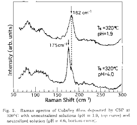 There is no Raman mode at 182
cm -1 in the ch-type CuInSe2 and this peak is strong for films exhibiting no
ch-XRD line. Therefore, this peak is considered not to be the chalcopyrite
mode but to be a phonon mode in the sphalerite lattice with disordered cation
atoms. This peak may be the same as an unidentified peak (185 cm-1)
reported for the CuInSe2 films prepared by the selenization method at
relatively low selenization temperature (255).26) If the peak at 182 cm-1
is assumed to be a sphalerite Raman mode, the film (Ts=320, pH=4.0) whose
Raman spectrum is shown in the lower part of Fig. 5 is composed mainly of
the chalcopyrite structure although some part of the cations are disordered.
There is no report on the Raman spectra of the sphalerite-type CuInSe2,
because crystal preparation is very difficult. The crystal prepared by
water-quenching of the CuInSe2 ingot from 950 exhibited clear ch-XRD
lines, although it was expected to have the sphalerite phase (ô-phase) at
950 from the phase diagram.27) Therefore, the thin CuInSe2 films prepared
by the CSP are of great importance in the research of the CuInSe2 with
sphalerite phase. A weak XRD line at 25.1K is considered to be due to the
110 diffraction of the In2Se3 second phase. Sometimes, this line is observed
as a shoulder of the chalcopyrite 112 line at 26.5K. However for the CuInSe2
prepared by CSP, the lines at 25.3Kand 25.5K have been assigned to the
Cu2-xSe and Cu2Se phases, respectively.14) The extra diffraction lines
located near this angle have been assigned to the In2Se3 phase for the
selenized26,28) and the vacuum-evaporated29) films. In the present study,
the line at 25.1K is assigned to the In2Se3 phase because the line is strong
for the In-rich films with negligible In2O3 content although it is contrary to
the assignments and the explanations done by the Stanford University
group.14,18-20) This line has been observed for all of the films deposited
with unneutralized solution (Fig.4(a)) and some of the films (Ts =300 )
deposited with neutralized solution (Fig.4(b)). The intensity of this line
becomes weaker as Ts increases. It is noted that the films exhibiting this
In2Se3 phase do not show XRD lines unique to the chalcopyrite structure. The
formation of the sphalerite phase due to the presence of In2Se3 has also been
reported for the film prepared by the vacuum deposition30) and the
selenization31) methods. From these results, it can be said that the
CuInSe2 films deposited by CSP tend to have chalcopyrite structure at high
substrate temperature, and the neutralization of the spray solution enhances
the formation of the chalcopyrite phase.
There is no Raman mode at 182
cm -1 in the ch-type CuInSe2 and this peak is strong for films exhibiting no
ch-XRD line. Therefore, this peak is considered not to be the chalcopyrite
mode but to be a phonon mode in the sphalerite lattice with disordered cation
atoms. This peak may be the same as an unidentified peak (185 cm-1)
reported for the CuInSe2 films prepared by the selenization method at
relatively low selenization temperature (255).26) If the peak at 182 cm-1
is assumed to be a sphalerite Raman mode, the film (Ts=320, pH=4.0) whose
Raman spectrum is shown in the lower part of Fig. 5 is composed mainly of
the chalcopyrite structure although some part of the cations are disordered.
There is no report on the Raman spectra of the sphalerite-type CuInSe2,
because crystal preparation is very difficult. The crystal prepared by
water-quenching of the CuInSe2 ingot from 950 exhibited clear ch-XRD
lines, although it was expected to have the sphalerite phase (ô-phase) at
950 from the phase diagram.27) Therefore, the thin CuInSe2 films prepared
by the CSP are of great importance in the research of the CuInSe2 with
sphalerite phase. A weak XRD line at 25.1K is considered to be due to the
110 diffraction of the In2Se3 second phase. Sometimes, this line is observed
as a shoulder of the chalcopyrite 112 line at 26.5K. However for the CuInSe2
prepared by CSP, the lines at 25.3Kand 25.5K have been assigned to the
Cu2-xSe and Cu2Se phases, respectively.14) The extra diffraction lines
located near this angle have been assigned to the In2Se3 phase for the
selenized26,28) and the vacuum-evaporated29) films. In the present study,
the line at 25.1K is assigned to the In2Se3 phase because the line is strong
for the In-rich films with negligible In2O3 content although it is contrary to
the assignments and the explanations done by the Stanford University
group.14,18-20) This line has been observed for all of the films deposited
with unneutralized solution (Fig.4(a)) and some of the films (Ts =300 )
deposited with neutralized solution (Fig.4(b)). The intensity of this line
becomes weaker as Ts increases. It is noted that the films exhibiting this
In2Se3 phase do not show XRD lines unique to the chalcopyrite structure. The
formation of the sphalerite phase due to the presence of In2Se3 has also been
reported for the film prepared by the vacuum deposition30) and the
selenization31) methods. From these results, it can be said that the
CuInSe2 films deposited by CSP tend to have chalcopyrite structure at high
substrate temperature, and the neutralization of the spray solution enhances
the formation of the chalcopyrite phase.
3.2.2 Effect of Cu/In
It is well known that the composition ratio, Cu/In,
affects not only the electrical properties but also the structural ones. Four
series of CuInSe2 films have been deposited using the spray solution with
different Cu/In (0.8
Cu/In
1.4). These four series stand for the combination
of the preparation condition of two pH values (1.9 and 4.0) and two substrate
temperatures Ts (300 and 360 ). The XRD patterns for the films deposited
at Ts=300 for pH=4.0 are shown in Fig. 6.
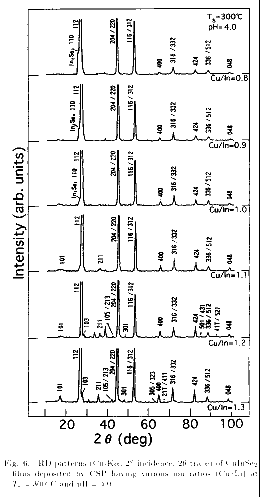 The In-rich films deposited at
Ts=300 exhibit no ch-XRD lines. Therefore, these films are considered to
have sphalerite structure. In such films, an XRD line due to the In2Se3 phase
can be seen at 25.1K. However, its intensity decreases as Cu/In increases.
In contrast, the Cu-rich films exhibited the chalcopyrite structure as
characterized by the appearance of the XRD lines, 101, 211 and 301,
independent of the pH value. At Ts=360 , both In- and Cu-rich films
exhibited the chalcopyrite structure, independent of pH. The XRD line due to
the In2Se3 phase (25.1K) can be seen for the In-rich films, similar to those
deposited at Ts=300 . From these results, it can be said that the Cu-rich
CuInSe2 films tend to have the chalcopyrite structure, whereas the In-rich
ones tend to have the sphalerite structure containing the In2Se3 phase. In Fig.
7, ranges of Cu/In and Ts for the production of the chalcopyrite and the
sphalerite phases are summarized for pH values of 1.9 and 4.0.
The In-rich films deposited at
Ts=300 exhibit no ch-XRD lines. Therefore, these films are considered to
have sphalerite structure. In such films, an XRD line due to the In2Se3 phase
can be seen at 25.1K. However, its intensity decreases as Cu/In increases.
In contrast, the Cu-rich films exhibited the chalcopyrite structure as
characterized by the appearance of the XRD lines, 101, 211 and 301,
independent of the pH value. At Ts=360 , both In- and Cu-rich films
exhibited the chalcopyrite structure, independent of pH. The XRD line due to
the In2Se3 phase (25.1K) can be seen for the In-rich films, similar to those
deposited at Ts=300 . From these results, it can be said that the Cu-rich
CuInSe2 films tend to have the chalcopyrite structure, whereas the In-rich
ones tend to have the sphalerite structure containing the In2Se3 phase. In Fig.
7, ranges of Cu/In and Ts for the production of the chalcopyrite and the
sphalerite phases are summarized for pH values of 1.9 and 4.0.
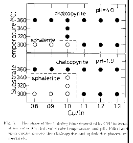
3.2.3 Formation of sphalerite and chalcopyrite phase
In the previous
subsection, it has been found that the CuInSe2 films deposited by CSP tend to
have the sphalerite phase rather than the chalcopyrite one when they were
deposited (i) at low Ts, (ii) with low pH spray solution, and (iii) with In-rich
spray solution, as can be seen in Fig. 7.
 The Ts effect on the sprayed
CuInSe2 film structure can be understood in terms the activation energy for
the formation of the respective phases. The spray pyrolysis is, in a sense,
regarded as a rapid quenching of the solute (reactant) after the solvent
evaporation. Since Cu and In ions are distributed at random in the spray
solution, the preferable quenched form is the sphalerite structure in which Cu
and In atoms are disordered in the cation sublattice. In order to form the
chalcopyrite structure, additional energy is required to order the atoms from
the disordered sphalerite form. This is the reason why the activation energy
for the chalcopyrite-phase formation (Ec) is larger than that for the
sphalerite one (Es). Therefore, the energy gained due to high Ts may enhance
the production of the chalcopyrite-type film. The films tend to exhibit
chalcopyrite structure when they have been deposited from the neutralized
solution. By analogy with the above discussion, the neutralization is
considered to decrease the activation energy Ec. The increase of pH, i.e., the
decrease of the H+ concentration, may enhance the following important
limiting reaction, in which the Cu2+ ion is reduced to Cu+ before it is
incorporated into CuInSe2. The reaction is represented as 32)
Cu2+(aq)+NH2(CH3)2NC=Se(aq) ´ Cu+(aq) + 1/2(NH(CH3)2-NC-Se)2(aq) + H+.
(1) It follows that the thermal decomposition reaction is enhanced, the
reaction of which is expressed as 32)
Cu2[NH2(CH3)2-NC-Se][CH3CH2OH]+(aq) + In3+(aq) + 4Cl-(aq) + 4H2O´
CuInSe2(s) + 2CO2(g) + 2(CH3)2NH(g) + 2NH3(g) + 4HCl(g) + CH3CH2OH(g).
(2) Therefore, the neutralization is considered to decrease the activation
energy for CuInSe2 formation, and both Ec and Es may decrease at the same
rate, causing the preferable formation of the chalcopyrite phase for the
neutralized solution. Similarly, the Cu-rich solution gives a high
concentration of Cu2+ ions, the effect being similar to the enhancement of the
reaction (1). This may decrease the activation energies in the same manner
as described above, causing the preferable formation of the chalcopyrite
phase for the Cu-rich solution.
The Ts effect on the sprayed
CuInSe2 film structure can be understood in terms the activation energy for
the formation of the respective phases. The spray pyrolysis is, in a sense,
regarded as a rapid quenching of the solute (reactant) after the solvent
evaporation. Since Cu and In ions are distributed at random in the spray
solution, the preferable quenched form is the sphalerite structure in which Cu
and In atoms are disordered in the cation sublattice. In order to form the
chalcopyrite structure, additional energy is required to order the atoms from
the disordered sphalerite form. This is the reason why the activation energy
for the chalcopyrite-phase formation (Ec) is larger than that for the
sphalerite one (Es). Therefore, the energy gained due to high Ts may enhance
the production of the chalcopyrite-type film. The films tend to exhibit
chalcopyrite structure when they have been deposited from the neutralized
solution. By analogy with the above discussion, the neutralization is
considered to decrease the activation energy Ec. The increase of pH, i.e., the
decrease of the H+ concentration, may enhance the following important
limiting reaction, in which the Cu2+ ion is reduced to Cu+ before it is
incorporated into CuInSe2. The reaction is represented as 32)
Cu2+(aq)+NH2(CH3)2NC=Se(aq) ´ Cu+(aq) + 1/2(NH(CH3)2-NC-Se)2(aq) + H+.
(1) It follows that the thermal decomposition reaction is enhanced, the
reaction of which is expressed as 32)
Cu2[NH2(CH3)2-NC-Se][CH3CH2OH]+(aq) + In3+(aq) + 4Cl-(aq) + 4H2O´
CuInSe2(s) + 2CO2(g) + 2(CH3)2NH(g) + 2NH3(g) + 4HCl(g) + CH3CH2OH(g).
(2) Therefore, the neutralization is considered to decrease the activation
energy for CuInSe2 formation, and both Ec and Es may decrease at the same
rate, causing the preferable formation of the chalcopyrite phase for the
neutralized solution. Similarly, the Cu-rich solution gives a high
concentration of Cu2+ ions, the effect being similar to the enhancement of the
reaction (1). This may decrease the activation energies in the same manner
as described above, causing the preferable formation of the chalcopyrite
phase for the Cu-rich solution.
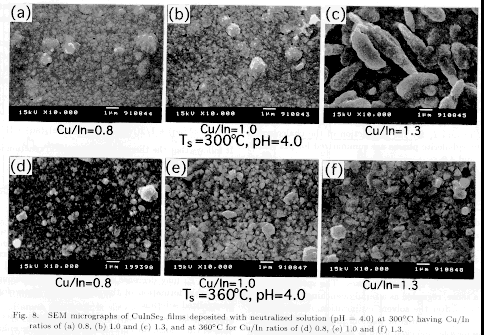
3.3 Surface morphology and film orientation
Figure 8 shows SEM images of
the surfaces of the sprayed CuInSe2 films (pH=4.0). In order to study the film
orientation, the X-ray diffraction patterns are shown in Figs. 9(a)-9(d), which
are measured using the conventional ó-2ó type goniometer. The general
trend observed from the SEM images is that the grain size is larger for (i)
larger Cu/In, (ii) higher Ts, and (iii) larger pH. The effect of Cu/In can be
clearly seen for films deposited at pH=4.0 and Ts=360 . As can be seen in
Figs. 8(d)`(f), the grain sizes increase with Cu/In, and they are 0.1`0.3, 0.3
`0.5 and 0.5`1.0 òm for Cu/In of 0.8, 1.0 and 1.3, respectively. As regards
the film orientation, the degree of 112 orientation increases with Cu/In,
which can be seen as the increase of the XRD intensity of the 112 line and the
disappearance of the relative intensities of the 220/204 and the 116/312
lines, as shown in Fig.9(d). This tendency is similar to that reported for other
deposition techniques. For the stoichiometric films (Cu/In=1.0), grains are
not well defined particularly for the films grown at 300 from the
unneutralized solution (pH=1.9), due to very small grain size (data not shown).
When the solution is neutralized (pH=4.0), grain size increases (about 0.1`
0.2 òm) as can be seen in Fig. 8(b).
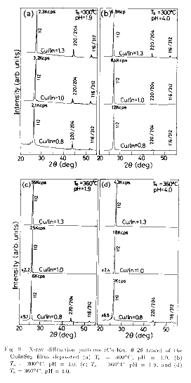 This can also be seen as the increase of
the 112 preferred orientation with pH, i.e., increase in intensity of the 112
line and the decrease in the relative intensities of 220/204 and 116/312
lines, as shown in the middle curves of Figs. 9(a) and 9(b). Similarly for the
Ts of 360, grain size increases from about 0.2 to 0.4 òm when pH is changed
from 1.9 to 4.0. The results are summarized as follows in view of the film
orientation deduced from the X-ray diffraction pattern shown in Fig.9. At Ts
of 300 , (i) the preferred 112 orientation is weak, and is shown together
with the 220/204 and 116/312 lines and the relatively weak 112 intensities
(2-10 kcps), (ii) the film orientation is slightly affected by Cu/In, and (iii)
the preferred 112 orientation increases with neutralization. At Ts of 360
, (i) intensity of the 112 line is stronger than that of the film grown at 300
by one order of magnitude, (ii) the XRD pattern is almost independent of pH,
and (iii) the film orientation exhibited a strong dependence on Cu/In as can be
seen in the monotonic increase of the intensity of the 112 line. These
tendencies observed in the film orientation are in good agreement with the
surface morohology observed by SEM. It has been reported by Brown and
Bates22) that the CuInSe2 films prepared by CSP on both the Mo-coated glass
and the glass substrates at Ts of 250 do not exhibit the columnar structure
typically found in CuInSe2 films grown by the other techniques,33) but exhibit
a fairly dense and planar layer with the rodlike grains on top. However, most
films grown in this study exhibited the columnar structure. Only a part of the
films grown from the Cu-rich solution at Ts of 300 exhibited the porous
morphology with rodlike grains as shown in Fig. 8(c), similar to the report of
Brown and Bates.22) Substrate temperature Ts used in this study was 300
Ts
360 , and is higher than that used by them. This may be the main
reason that the surface morphology obtained in this study is very different
from that obtained by Brown and Bates. As shown in Fig.8(e) and 8(f), the
films deposited at Ts of 360 from the stoichiometric and Cu-rich solutions
are characterized by large grains. Such films are found to be highly oriented
to 112, as has been discussed above and can be seen in the top and the middle
curves in Figs.9(c) and 9(d), in which only one intense 112 XRD peak has been
observed in the ó-2ó trace. These X-ray results indicate that the
well-developed grains with the size of 0.2`0.5 òm observed in such films are
oriented to 112, and the film is considered to have a fibous texture.
This can also be seen as the increase of
the 112 preferred orientation with pH, i.e., increase in intensity of the 112
line and the decrease in the relative intensities of 220/204 and 116/312
lines, as shown in the middle curves of Figs. 9(a) and 9(b). Similarly for the
Ts of 360, grain size increases from about 0.2 to 0.4 òm when pH is changed
from 1.9 to 4.0. The results are summarized as follows in view of the film
orientation deduced from the X-ray diffraction pattern shown in Fig.9. At Ts
of 300 , (i) the preferred 112 orientation is weak, and is shown together
with the 220/204 and 116/312 lines and the relatively weak 112 intensities
(2-10 kcps), (ii) the film orientation is slightly affected by Cu/In, and (iii)
the preferred 112 orientation increases with neutralization. At Ts of 360
, (i) intensity of the 112 line is stronger than that of the film grown at 300
by one order of magnitude, (ii) the XRD pattern is almost independent of pH,
and (iii) the film orientation exhibited a strong dependence on Cu/In as can be
seen in the monotonic increase of the intensity of the 112 line. These
tendencies observed in the film orientation are in good agreement with the
surface morohology observed by SEM. It has been reported by Brown and
Bates22) that the CuInSe2 films prepared by CSP on both the Mo-coated glass
and the glass substrates at Ts of 250 do not exhibit the columnar structure
typically found in CuInSe2 films grown by the other techniques,33) but exhibit
a fairly dense and planar layer with the rodlike grains on top. However, most
films grown in this study exhibited the columnar structure. Only a part of the
films grown from the Cu-rich solution at Ts of 300 exhibited the porous
morphology with rodlike grains as shown in Fig. 8(c), similar to the report of
Brown and Bates.22) Substrate temperature Ts used in this study was 300
Ts
360 , and is higher than that used by them. This may be the main
reason that the surface morphology obtained in this study is very different
from that obtained by Brown and Bates. As shown in Fig.8(e) and 8(f), the
films deposited at Ts of 360 from the stoichiometric and Cu-rich solutions
are characterized by large grains. Such films are found to be highly oriented
to 112, as has been discussed above and can be seen in the top and the middle
curves in Figs.9(c) and 9(d), in which only one intense 112 XRD peak has been
observed in the ó-2ó trace. These X-ray results indicate that the
well-developed grains with the size of 0.2`0.5 òm observed in such films are
oriented to 112, and the film is considered to have a fibous texture.
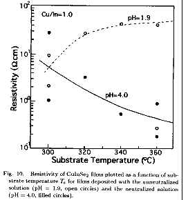
3.4 Resistivity
All the CuInSe2 films deposited by CSP exhibited p-type
conductivity, similarly to the previous reports.11,16,17,20) The Hall voltage
was too small to be measured. Therefore, the hole mobility is considered to
be smaller than 1 cm2/Vs, similar to the previously reported values for the
CSP films.8,16) Figure 10 shows the film resistivity plotted as a function
of Ts. The films have been deposited from the unneutralized (pH=1.9) and
neutralized (pH=4.0) spray solutions with the stoichiometric molar ratio
(Cu/In=1.0). The film resistivity increases with Ts for the unneutralized
solution (pH=1.9), while it decreases with Ts for the neutralized solution
(pH=4.0).
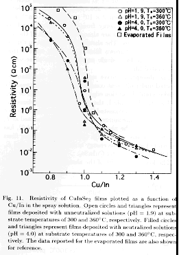 Figure 11 shows resistivity plotted as a function of Cu/In in the
spray solution for the four series of CuInSe2 films which have been deposited
at different pH (pH=1.9 or 4.0) and Ts (Ts=300 or 360 ) values. The result
for the three-source-evaporated CuInSe2 films is also shown.34) For all the
films, resistivity exhibits a drastic decrease by about six orders of magnitude
when Cu/In increases from 0.8 to 1.3. This result agrees well with the
previously reported resistivity change.17,20) All the In-rich films (0.8
Cu/In
0.9) exhibited the high resistivities of 102`3x10⁴Ñcm. This high
resistivity has been explained by both the decrease of the number of acceptors
(CuIn) and the compensation of acceptors with donors (InCu).32) In this
In-rich region, several changes in resistivity depending on the growth
condition have been observed: (i) the effect of Ts is small for films sprayed
with unneutralized solution (pH=1.9), (ii) film resistivity for the neutralized
solution (pH=4.0) is lower than that for the unneutralized solution by one to
two orders of magnitude, and (iii) resistivity for the film deposited using the
neutralized solution (pH=4.0) at Ts of 360 is lower than that for pH=4.0 at
Ts of 300 . The lower resistivity of the films for both higher pH and higher
Ts is considered to be mainly due to the larger hole mobility caused by the
improved crystal quality of the film (pH=4.0, Ts=360), although the mobility
has not yet been measured. The finding that the slope of the curve (0.9
Cu/In
1.0) is less steep for the neutralized solution (pH=4.0) than for the
unneutralized solution (pH=1.9) indicates the superiority of the neutralized
solution in controlling resistivity. However, the resistivity of the Cu-rich
film is almost the same at around 10-2-10-1 Ñcm for the four curves. This
low resistivity is comparable to that reported for the three-source
evaporation method,34) and the main reason for this is the current flowing in
the low-resistive Cu2-xSe second phase that precipitated in the grain
boundary. In fact, a weak diffraction line due to Cu2-xSe at about 32K has
been observed for the Cu-rich film (Cu/In1.2). Therefore, the low resistivity
of the Cu-rich film may be related to the Cu2-xSe phase.
Figure 11 shows resistivity plotted as a function of Cu/In in the
spray solution for the four series of CuInSe2 films which have been deposited
at different pH (pH=1.9 or 4.0) and Ts (Ts=300 or 360 ) values. The result
for the three-source-evaporated CuInSe2 films is also shown.34) For all the
films, resistivity exhibits a drastic decrease by about six orders of magnitude
when Cu/In increases from 0.8 to 1.3. This result agrees well with the
previously reported resistivity change.17,20) All the In-rich films (0.8
Cu/In
0.9) exhibited the high resistivities of 102`3x10⁴Ñcm. This high
resistivity has been explained by both the decrease of the number of acceptors
(CuIn) and the compensation of acceptors with donors (InCu).32) In this
In-rich region, several changes in resistivity depending on the growth
condition have been observed: (i) the effect of Ts is small for films sprayed
with unneutralized solution (pH=1.9), (ii) film resistivity for the neutralized
solution (pH=4.0) is lower than that for the unneutralized solution by one to
two orders of magnitude, and (iii) resistivity for the film deposited using the
neutralized solution (pH=4.0) at Ts of 360 is lower than that for pH=4.0 at
Ts of 300 . The lower resistivity of the films for both higher pH and higher
Ts is considered to be mainly due to the larger hole mobility caused by the
improved crystal quality of the film (pH=4.0, Ts=360), although the mobility
has not yet been measured. The finding that the slope of the curve (0.9
Cu/In
1.0) is less steep for the neutralized solution (pH=4.0) than for the
unneutralized solution (pH=1.9) indicates the superiority of the neutralized
solution in controlling resistivity. However, the resistivity of the Cu-rich
film is almost the same at around 10-2-10-1 Ñcm for the four curves. This
low resistivity is comparable to that reported for the three-source
evaporation method,34) and the main reason for this is the current flowing in
the low-resistive Cu2-xSe second phase that precipitated in the grain
boundary. In fact, a weak diffraction line due to Cu2-xSe at about 32K has
been observed for the Cu-rich film (Cu/In1.2). Therefore, the low resistivity
of the Cu-rich film may be related to the Cu2-xSe phase.
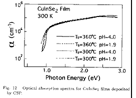
3.5 Optical absorption
Figure 12 shows the optical absorption spectra for
the stoichiometric CuInSe2 films sprayed with the neutralized (pH=4.0) and
unneutralized (pH=1.9) solutions at different substrate temperatures (Ts=300
and 360 ). Films exhibited an abrupt increase of the absorption coefficient
at about 1.0 eV which is close to the band gap (Eg) of 1.02 eV at 300 K for the
bulk CuInSe2 crystal. 35) Above Eg, the absorption coefficient exhibited
gradual increase from 2 x 10⁴ to 1.5 x 105 cm-1 with increasing photon energy
from 1.1 to 3.0 eV, and the spectra in this region are almost independent of
the film growth conditions. The absorption coefficient in this region of the
CSP-grown films is, however, smaller than those for the bulk single crystal
and the three-source evaporated film.2) The absorption curves are different
for the films deposited under different conditions in the region near the
fundamental absorption edge (0.9`1.1 eV), as can be seen in Fig. 12. In Table
I, the energies of the fundamental absorption edge estimated by the linear
extrapolation of the ¢2-hù plot are summarized. The film deposited at Ts of
360 from the neutralized solution (pH=4.0), has the highest absorption edge
(1.01 eV) among four films shown in Fig. 12. This energy is close to the
reported Eg of 1.02 eV for the bulk CuInSe2. The low-energy shift of the
absorption edge has been observed for films deposited at Ts of 300 . The
absorption edges of the films deposited using the unneutralized (pH=1.9) and
the neutralized (pH=4.0) solutions are 0.94 and 0.95 eV, respectively. This
energy shift may be related to the film structure being sphalerite rather than
chalcopyrite, although Eg of the sphalerite CuInSe2 is not known yet. 4.
Conclusions CuInSe2 polycrystalline films have been systematically grown
by the chemical spray pyrolysis method. Studies have been made with respect
to substrate temperature, ion ratio (Cu/In) and pH of the spray solution. Films
have been characterized by X-ray, SEM, Raman, resistivity and optical
absorption methods. The main conclusions obtained in this study are as
follows. (i) All films deposited by CSP exhibited p-type conductivity, (ii)
films deposited at high Ts and those deposited at a high pH solution led to the
production of the chalcopyrite phase, while those deposited at low Ts and low
pH led to the production of sphalerite films, (iii) films deposited using the
In-rich solution had the sphalerite structure with the In2Se3 second phase,
while films deposited using the Cu-rich solution exhibited the chalcopyrite
structure, (iv) film resistivity changed from 10-2 to 10 5 Ñcm when Cu/In
was changed from 1.3 to 0.8, (v) increase in Ts and pH increased the grain size,
and (vi) films deposited at high Ts exhibited the (112) textured columnar
growth. Finally, we conclude that good chalcopyrite CuInSe2 films with
large grains can be grown using the neutralized spray solution (pH=4) at the
growth temperature of 360.
Acknowledgments
                       The authors would like to thank Messrs. K. Takemura and
 A. Fujisawa of Central Research Laboratory, Nippon Sheet Glass Co., Ltd., for
 supplying the spray nozzle.  The authors would also like to thank Mr. A. Miyata
 for SEM measurements and Dr. S. Chichibu and Mr. R. Sudo of the Faculty of
Science and Technology, Keio University, for X-ray diffraction measurements.